
PCB Fabrication
What is PCB Fabrication?
PCB fabrication is the process of manufacturing printed circuit boards (PCBs) used in electronic
devices. It involves transforming design specifications into physical circuit boards through
various manufacturing processes.
How does PCB Fabrication work?
Design Preparation : Design specifications are prepared in Gerber format, detailing the
layout,
traces, and components of the PCB.
Substrate Processing : Substrate Processing: Substrate materials, typically
fiberglass-reinforced epoxy laminate, are
prepared for PCB fabrication.
Layer Assembly : Individual layers of substrate with copper foil are aligned and
laminated
together to form the PCB structure, especially for multi-layer PCBs.
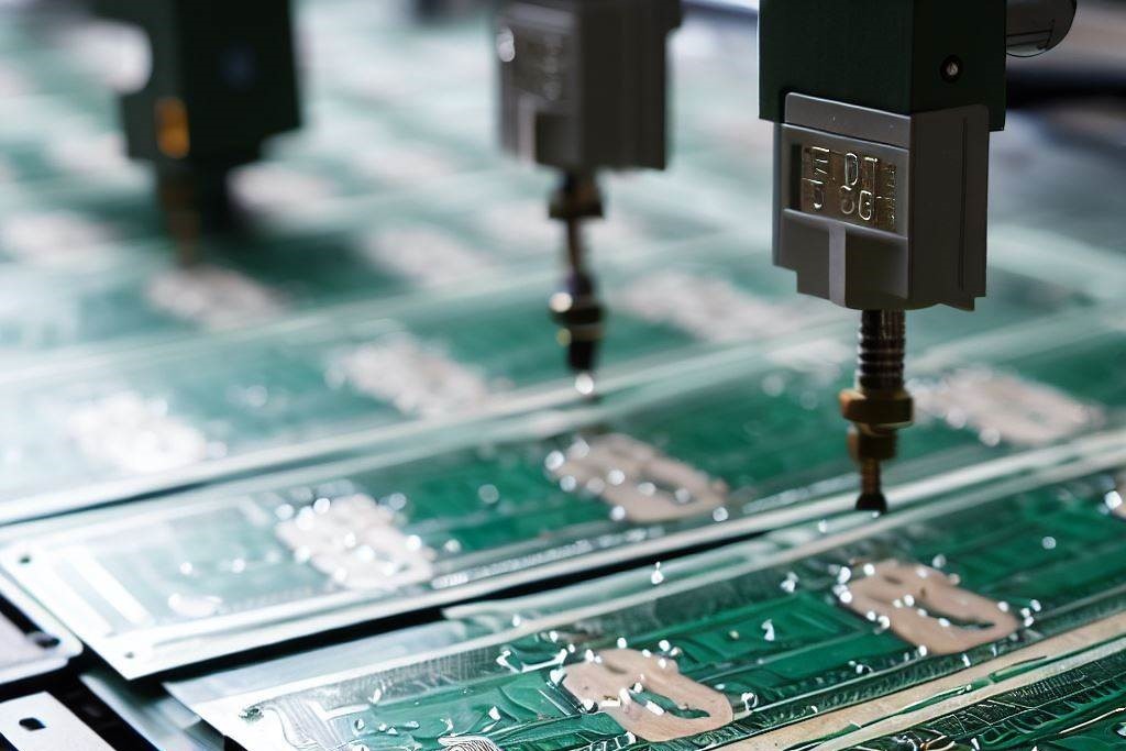
Circuit Formation : Copper traces are created on the substrate through processes like
photoresist application, etching, drilling, and plating to achieve the desired circuit pattern.
Finishing Touches : Surface finish, silkscreen printing, and testing/inspection are
applied to
ensure the quality, reliability, and functionality of the fabricated PCBs.
Why Choose Neural Circuits for your PCB Fabrication?

Quality Assurance :
We adhere to stringent quality standards throughout the PCB fabrication process, ensuring the
reliability and performance of your PCBs.

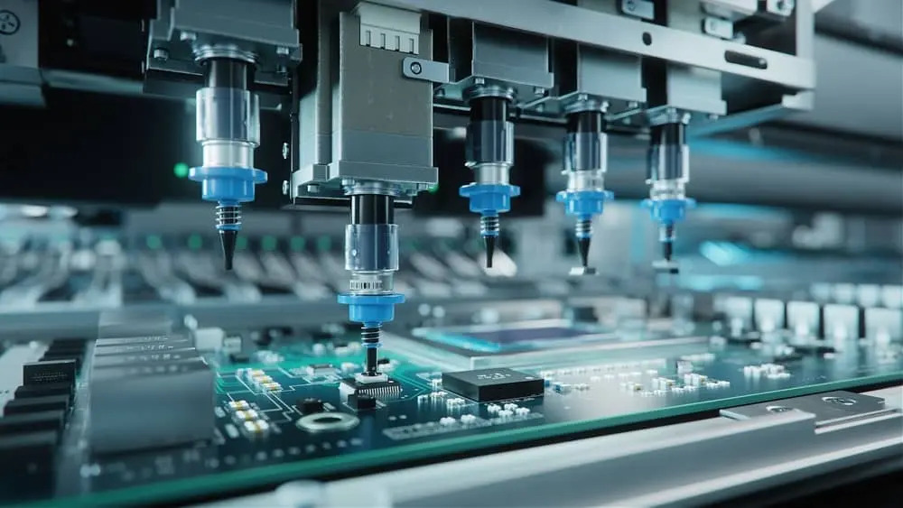
Advanced Manufacturing Technology :
Our state-of-the-art manufacturing facility is equipped with advanced technology and machinery
for precise and efficient PCB fabrication.

Customized Solutions :
We offer customization options to meet your specific requirements, including choice of substrate
material, surface finish, and PCB thickness.

Timely Delivery :
We are committed to delivering your PCBs on time, helping you meet project deadlines and
objectives.

Cost-Effective :
Despite our commitment to quality, we offer competitive pricing for PCB fabrication services,
ensuring excellent value for your investment.